Hardware Documentation:
BayCom RS-232 modem


Important Advice:

Text, Designs and Circuits in this manual are copyright protected. Also an abstract circulation and publication is only permitted with the previous written consent of the authors. Manual may be copied only for private purposes.

Liability Disclaimer: The authors undertake no responsibility for the correctness of the published circuits and other directions as well as the technical description. They are not responsible in the case of damage which originates from the construction or insertion of the described circuit, of the kit or completed modem. The user is responsible for proper operation corresponding to the national laws.

The copyright for the circuit and the original manual are with
Johannes Kneip
DG3RBU
Bert-Brecht-Weg 28
30890 Barsinghausen
GERMANY


The english translation has been done by Johannes Kneip and Denis Godfrey, G0KIU.

The BayCom - Team likes to thank Denis, G0KIU and Phil, G6IIM for their kind help and efforts to support BayCom in the United Kingdom.

Documentation for the Serial Modem


The described modem is a an interface for packet radio operation with 1200 Bd on amateur radio VHF/UHF bands. The modem is constructed by using the highly integrated Texas-Instruments modem chip TCM3105. This IC consumes so less power, that it can be supplied from the RS-232 signal lines. The modem can additionally be equipped with an optional "Carrier-Detect" hardware, which analyzes incoming audio for proper packet radio signals. The optional DCD is also described in this manual.

The Circuit

The modem stems in principle from the customary TCM3105 circuitry, the corresponding COM ports adaptions have beend added. The schematics (on seperate page) consists of four blocks: In the left upper corner, the COM adaptions and the power supply can be seen, in the right upper corner the modem circuitry itself is drawn. In the right lower corner the PTT circuitry with a watchdog can be seen. The optional DCD circuitry is in the left lower corner.
The modems draws the required current from the RS-232-COM port via the diodes D1-D3. In RECEIVE mode, there is approx. 12V at the DTR line, in the SEND modem RTS lies at 12V, additionally an irregular clock will be used that is created at TXD by the RS-232 programming. These three voltage supplies arrive via D1-D3 at the zener diode stabilizer (R17, D6) generating the required +5V. C1 and C2 serve as smoothing and reservoir.
The levels of the RS-232-COM port are not compatible with the CMOS ICs used by us. Therefore, for us it is required to adjust the level from -15V to +15V to that of our employed TTL logic. This occurs through the CMOS inverters 2A and 2B and associated current limiting resistors R1 - R3. An acknowledged somewhat unorthodox method, but which saves the expense of dearer special IC as MAX 232 and up to now has given no problems. It is certainly necessary to use a 74HC04 or 74HC14 for IC2, other types do not function properly! To generate the negative RS-232 levels, we use the negative voltage from the RS-232 as source. Data coming from the modem IC activate a PNP transistor. This transistor switches positive level to the RECEIVE line CTS. If not activated, R9 forces CTS to the low level of -12V on RTS during RECEIVE.


Circuitry of the Serial Modem


The PTT will be switched by T1. R4, R5, C3 and D4 construct a watchdog timer, which switches off the PTT after approximately 60 secs of being keyed (important with a possible program crash). The actual conversion of the data into modulation capable of being sent and returned will be undertaken by the adequate modem IC TCM3105, which is also set for Bell norm 202 at pins 2, 5, 12 and 13, which is customary norm for VHF/UHF. The clock generation for the TCM3105 occurs from Q1.
The SEND signal is passed to the Mic entry of the transceiver via C7, R15, R11, R13 and C8. R11 serves to adjust the amplitude. On the receiving side, the AF is gained from the speaker output of the radio. In the modem, R10, D7 and D8 limit the AF level to 0.7V, which are fed to the modem IC.

The optional DCD is constructed with the PLL integrated circuit XR211 by EXAR. By the arrangement as a double tone decoder, this noise barrier addresses itself only to PR signals, other disturbances (e.g. ISM signals) do not represent received data of the modem, which without the squelch has been the case. The arriving signal will be tapped of at the input of the TCM3105 and coupled via C21 to the input of the PLL IC. The external switching of the IC determines the wait delay of the noise barrier. The double tone decoder occupies a centre frequency of 1700 Hz (with the Bell 202 norm, which is employed in amateur radio, the values 1200/2200 Hz are defined as mark and space, (1200 + 2200)/2 gives the center frequency of 1700 Hz), which can be installed by C22, R22 and R24. The bandwith (tracking frequency), to which the squelch reacts, is set with R23, this must amount exactly the 2*500Hz above and below the centre, along with the "arched" resistance of 43 kOHms. C23 determines the damping factor of the PLL. C20 and R21 are for the capture frequency condition, therefore the maximum deviation from the theoretical spot frequencies 1200 and 2200 Hz by which the PLL now occupies.
If the PLL is not at rest, output 6 of the XR2211 is low and T3 cannot be switched by the data of the TCM3105. If the PLL is at rest, the low-level at the XR2211 disappears (this is an open collector output, which occupies no defined "High"-level), therefore the data of the TCM3105 can be utilised by the computer.


Construction


The modem itself and the DCD are assembled on two different PCBs. If the DCD is used, the TCM3105 is not inserted in the modem socket, but in the socket on the DCD board. The DCD board has a connector at it's solder side, fitting in the modem-IC socket on the modem PCB, so it is an "above-board" for the modem. Due to this, both PCBs are assembled seperately.

Parts list modem


R1   100k                        D1  1N4148
R2   100k                        D2  1N4148
R3   2k2                         D3  1N4148
R4   100k                        D4  1N4148
R5   2M2                         D5  1N4148
R6   10k                         D6  ZPD 5.1
R7   15k                         D7  1N4148
R8   33k                         D8  1N4148
R9   15k             
R10   1k                         T1  BC548
R11   Trim Pot, 10k horizonal    T2  BC548
R12   1k                         T3  BC558
R13   10k
R14   12k                        IC1 TCM3105
R15   10k                        IC2 74HC04
R16   10k
R17   120                        Q 1 Crystal 4.4336 MHz
                                
C1  100 mF Elyt,                 St1 9way socket D-sub female
C2  10 mF Elyt,                  St2 5way. DIN-socket
C3  10 mF Elyt,         
C4  27p ceramic,                 14 pin IC-socket 
C5  27p ceramic,                 16 pin IC-socket
C6  100n metallic,               PCB serial modem
C7  100n metallic,  
C8  100n metallic 

Hardware DCD (optional)

R20   3k9                        C20   150n metallic
R21   470k                       C21   100n metallic
R22   18k                        C22   22n metallic
R23   43k                        C23   4,7n metallic
R24   Trim Pot. 10k horizontal   C24   100n metallic

IC20  XR2211                     16-pin IC socket
                                 16-pin IC socket
                                 IC-connector 16 pin
                                 PCB hardware DCD
At first, all lower components as resistors, diodes and IC sockets are mounted and soldered. For the ICs precision sockets should be used to avoid corrosion problems and to make it easier to insert the hardware DCD in the TCM3105-socket lateron. On the DCD board, take care of the different orientation of the sockets for the XR2211 and the TCM3105. The TCM3105 socket is inserted in the row of holes closer to the XR2211, the other holes are used for the connector to the
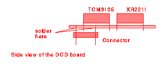
 modem board.
Then, the other components as capacitors, trims, transistors and connectors can be assembled and soldered. On the DCD-board, the connector to the modem board is also soldered now. It looks like an IC socket, but has pins on both sides. The thicker pins are now soldered to the pads on the DCD board from the solder side of the PCB, see drawing below:


As soon as the assembly is finished, the ICs are inserted into the sockets. The TCM3105 is inserted in the modem PCB, when the DCD is not used, and it is inserted on the DCD board, which itself is inserted in the TCM3105 socket on the modem board. Please take care of the different orientation of the ICs on the DCD board again!

(Assembly: See seperate File)

Connections to the radio and to the computer


The modem posses a 9-way Sub-D connector for the RS-232-port of the computer. A 1:1 cable can be used to connect the modem to the RS-232 port. The following lines are used:


Signal      Pin       Function          Signal      Pin       Function
DTR         4       Transmit Data       RTS         7   PTT (High-Active)
CTS         5       Receive Data        TXD         2   Power supply
GND         7       Ground                            
If you have a 25-way connector at your RS-232 port instead of a 9-way connector, you have to assemble an adapter cable as follows:
25 way connector        connect with 9-way connector
TXD   Pin 2                 Pin 3
DTR   Pin 20                Pin 4
CTS   Pin 5                 Pin 8
RTS   Pin 4                 Pin 7
GND   Pin 7                 Pin 5
The connection to the radio is made via a 5 way DIN socket. It is used as follows:


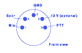
Connect Spkr with the speaker output of the radio. The modem has an input impedance of about 1 kOhms, if you have a speaker output with very low impedance, you should add an additional load (about 100 Ohms) to achieve a good adaption of the modem to the output. If you have an output with high impedance, no special measures are required.

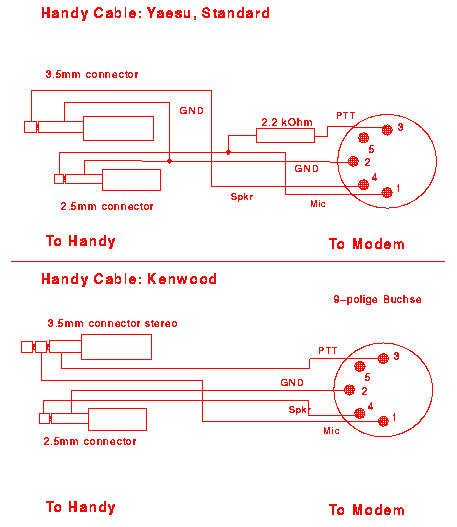
Connect Mic with the microphone input of the radio, also the PTT output with the PTT input of the radio. Do not forget to connect the modem ground to the radio ground. The +12V line is only used in the case, that the modem cannot be power-supplied via the RS-232 port. If you use a handy without seperated PTT-connector, you have to assemble a special cable for it. For these handies, the PTT switching is provided by a 2.2 kOhms resistor, forcing a DC-current on the MIC line. The following figure shows some examples for handy cables. Please consult you handy manual about the connections to be made!


Implementation and Alignment


When the PCB has all of the Components in position and soldered, the solder side of the board should be carefully checked for shorts between the tracks. This is especially necessary in the region of the COM Port connections. A short here can cause damage to the Computer Hardware.
When you are sure that there are no solder bridges, short circuits or broken tracks/dry joints etc. on the PCB, the Modem should be connected to the RS232 Port and L2 Started. It is absolutely necessary for L2 to be running or there will be no voltage supply to the PCB. (A transceiver should not be connected at this time). After L2 has been started a flashing rectangle will appear in the top right hand corner of the screen, unless there is a software problem. (see software manual).

Voltage Checks.

Now the voltage (Pin 14 (+5V) -Earth) on IC2 should be measured. If this lies approximately at 5 Volts (+/- 0.2V) the power supply works ok and the following paragraphs should be carried out.
Prove whether pin 7 of the TCM3105 has a voltage between 2.6 and 2.8 (ideal value 2.7) If the value lies outside this tolerance, the potential divider R6/R14 should be altered. If the Voltage is to high R14 should be increased, if it is too low then reduce R14.
The Send Signals should be adjusted with R11. Install a long TXDELAY (for the practical testing) and send a test packet. (e.g. UNPROTO by pressing return on the F10 Screen - SCC should be running !). Now R11 should be so installed, that the individual signal appears somewhat similar to the other signals on the frequency. It is important that the volume is not too loudly modulated, otherwise it causes the signal to be un-decodable.A further possibility for the checking is as follows: Start with the pot. at minimum modulation, while monitoring with another RX slowly increase the modulation by adjusting the trim pot. until the sound ceases to increase in volume, in other words, remains constant. Now the most useful value for the installation is slightly below halfway between the minimum value and the position where the sound failed to increase in volume. (I have found another suitable set up procedure which is as follows: with the Pot. set to minimum, try to connect to a NODE or a friend by arrangement. Turn the Pot in steps, pausing between steps until a connect is made, then give the Pot. a slight tweak more and it should be OK for use. G0KIU)


Now the setting for the squelch control should be installed, when the optional DCD board is used. Switch off software carrier detection (mode parameter in the software!). The squelch should be opened and R24 set so that with noise at the input, the QRV indicator in the status line of BayCom switches every 0.5-1 seconds (approx.) briefly to EMPF. If there is a PR-Signal present, EMPF remains for the duration of the signal. According to the requirement the squelch can be adjusted finely with R24. We do not think that it is necessary to use a function generator for this purpose.

Now all the alignment procedures are finished and normal PR operation can be started. Do not forget to reduce TXDELAY to a suitable value again!


Technical Data:

Input Impedance AF:       1kOhm
Output Impedance:         approx. 10 kOhm
Board dimensions:         88 * 46 * 23 mm


(Help) (Home) (Up)